Metodo di pagamento


4-By-4 Register Files With 3-State Outputs
FP16Produttore:
ProduttorePart #:
7704201FA
Scheda dati:
Supply Voltage (min) (V):
4.75
Supply Voltage (max) (V):
5.25
Input Type:
Bipolar
Output Type:
3-State
Invia tutte le distinte materiali a ![]() [email protected],
oppure compila il modulo sottostante per un preventivo su 7704201FA. Risposta garantita entro
[email protected],
oppure compila il modulo sottostante per un preventivo su 7704201FA. Risposta garantita entro
![]() 12hr.
12hr.
Compila il breve modulo sottostante e ti forniremo immediatamente il preventivo.
The SN54LS670 and SN74LS670 MSI 16-bit TTL register files incorporate the equivalent of 98 gates. The register file is organized as 4 words of 4 bits each and separate on-chip decoding is provided for addressing the four word locations to either write-in or retrieve data. This permits simultaneous writing into one location and reading from another word location.
Four data inputs are available which are used to supply the 4-bit word to be stored. Location of the word is determined by the write-address inputs A and B in conjunction with a write-enable signal. Data applied at the inputs should be in its true form. That is, if a high-level signal is desired from the output, a high-level is applied at the data input for that particular bit location. The latch inputs are arranged so that new data will be accepted only if both internal address gate inputs are high. When this condition exists, data at the D input is transferred to the latch output. When the write-enable input, G\W, is high, the data inputs are inhibited and their levels can cause no change in the information stored in the internal latches. When the read-enable input, G\R, is high, the data outputs are inhibited and go into the high-impedance state.
The individual address lines permit direct acquisition of data stored in any four of the latches. Four individual decoding gates are used to complete the address for reading a word. When the read address is made in conjunction with the read-enable signal, the word appears at the four outputs.
This arrangement — data-entry addressing separate from data-read addressing and individual sense line — eliminates recovery times, permits simultaneous reading and writing, and is limited in speed only by the write time (27 nanoseconds typical) and the read time (24 nanoseconds typical). The register file has a nondestructive readout in that data is not lost when addressed.
All inputs except read enable and write enable are buffered to lower the drive requirements to one Series 54LS/74LS standard load, and input-clamping diodes minimize switching transients to simplify system design. High-speed, double-ended AND-OR-INVERT gates are employed for the read-address function and have high-sink-current, three-state outputs. Up to 128 of these outputs may be bus connected for increasing the capacity up to 512 words. Any number of these registers may be paralleled to provide n-bit word length.
The SN54LS670 is characterized for operation over the full military temperature range of -55°C to 125°C; the SN74LS670 is characterized for operation from 0°C to 70°C.


| Supply voltage (min) (V) | 4.75 | Supply voltage (max) (V) | 5.25 |
| Input type | Bipolar | Output type | 3-State |
| Clock frequency (max) (MHz) | 35 | Features | Unidirectional |
| Operating temperature range (°C) | -55 to 125 | Rating | Military |
| feature-logic-family | LS | feature-logic-function | Register File |
| feature-number-of-channels-per-chip | 4 | feature-number-of-elements-per-chip | 1 |
| feature-number-of-element-inputs | 4 | feature-number-of-element-outputs | 4 |
| feature-polarity | Non-Inverting | feature-triggering-type | |
| feature-process-technology | Bipolar | feature-output-type | 3-State |
| feature-maximum-low-level-output-current-ma | 4 | feature-maximum-high-level-output-current-ma | -1 |
| feature-minimum-operating-supply-voltage-v | 4.5 | feature-maximum-operating-supply-voltage-v | 5.5 |
| feature-packaging | Tube | feature-rad-hard | No |
| feature-pin-count | 16 | feature-cecc-qualified | No |
| feature-esd-protection | feature-escc-qualified | ||
| feature-military | Yes | feature-aec-qualified | No |
| feature-auto-motive | No | feature-p-pap | No |
| feature-eccn-code | EAR99 | feature-svhc | Yes |
| feature-svhc-exceeds-threshold | Yes |
Relativi al servizio post-vendita e alla liquidazione
 Pagamento
Metodo di pagamento


Per canali di pagamento alternativi, contattaci a:
[email protected] Spedizione e imballaggio
metodo di spedizione


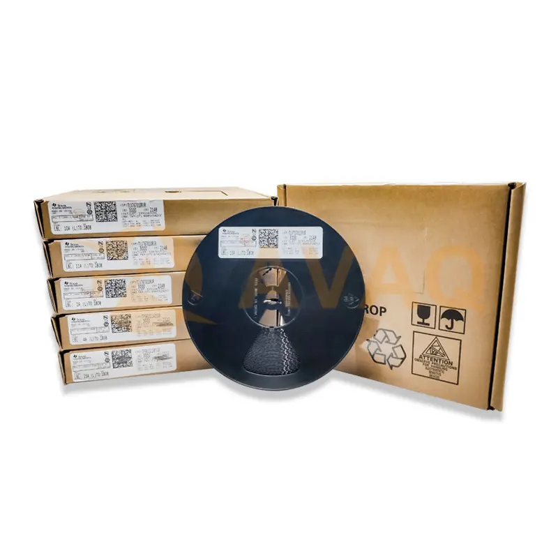
AVAQ determina e confeziona tutti i dispositivi in base ai requisiti di protezione contro le scariche elettrostatiche (ESD) e il livello di sensibilità all'umidità (MSL)..
 Garanzia

Prodotto 365 giorni
Qualità garantita
Promettiamo di fornire un servizio di garanzia della qualità di 365 giorni per tutti i nostri prodotti.
| Qtà. | Prezzo unitario | Est. Prezzo |
|---|---|---|
| 1+ | - | - |
I prezzi sottostanti sono solo di riferimento.