Metodo di pagamento


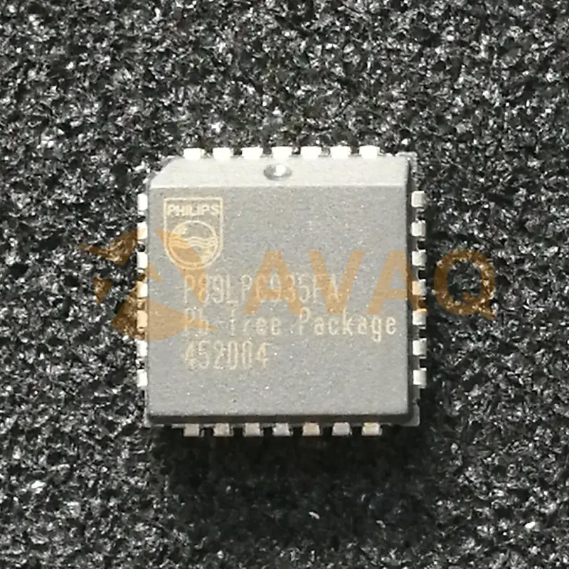
The P89LPC935FA Microcontroller IC from the 8051 series offers 8KB of FLASH memory, operates at 12MHz, and comes in a 28-PLCC package
PLCC28Produttore:
ProduttorePart #:
P89LPC935FA
Scheda dati:
Pbfree Code:
Yes
Part Life Cycle Code:
Obsolete
Pin Count:
28
Reach Compliance Code:
compliant
EDA/CAD Modelli:
All bill of materials (BOM) can be sent via email to ![]() [email protected],
or fill below form to Quote for P89LPC935FA, guaranteed quotes back within
[email protected],
or fill below form to Quote for P89LPC935FA, guaranteed quotes back within
![]() 12hr.
12hr.
Compila il breve modulo sottostante e ti forniremo immediatamente il preventivo.
General descriptionThe P89LPC933/934/935/936 is a single-chip microcontroller, available in low cost packages, based on a high performance processor architecture that executes instructions in two to four clocks, six times the rate of standard 80C51 devices. Many system-level functions have been incorporated into the P89LPC933/934/935/936 in order to reduce component count, board space, and system cost.FeaturesPrincipal features■ 4 kB/8 kB/16 kB byte-erasable flash code memory organized into 1 kB/2 kB sectors and 64-byte pages. Single-byte erasing allows any byte(s) to be used as non-volatile data storage.■ 256-byte RAM data memory. Both the P89LPC935 and P89LPC936 also include a 512-byte auxiliary on-chip RAM.■ 512-byte customer data EEPROM on chip allows serialization of devices, storage of setup parameters, etc. (P89LPC935/936).■ Dual 4-input multiplexed 8-bit A/D converters/DAC outputs (P89LPC935/936, single A/D on P89LPC933/934).Two analog comparators with selectable inputs and reference source.■ Two 16-bit counter/timers (each may be configured to toggle a port output upon timer overflow or to become a PWM output) and a 23-bit system timer that can also be used as an RTC.■ Enhanced UART with fractional baud rate generator, break detect, framing error detection, and automatic address detection; 400 kHz byte-wide I2C-bus communication port and SPI communication port.■ Capture/Compare Unit (CCU) provides PWM, input capture, and output compare functions (P89LPC935/936).■ High-accuracy internal RC oscillator option allows operation without external oscillator components.The RC oscillator option is selectable and fine tunable.■ 2.4 V to 3.6 V VDD operating range. I/O pins are 5 V tolerant (may be pulled up or driven to 5.5 V).■ 28-pin TSSOP, PLCC, and HVQFN packages with 23 I/O pins minimum and up to 26 I/O pins while using on-chip oscillator and reset options. Additional features■ A high performance 80C51 CPU provides instruction cycle times of 111 ns to 222 ns for all instructions except multiply and divide when executing at 18 MHz. This is six times the performance of the standard 80C51 running at the same clock frequency. A lower clock frequency for the same performance results in power savings and reduced EMI.■ Serial flash In-Circuit Programming (ICP) allows simple production coding with commercial EPROM programmers. Flash security bits prevent reading of sensitive application programs.■ Serial flash In-System Programming (ISP) allows coding while the device is mounted in the end application.■ In-Application Programming (IAP) of the flash code memory. This allows changing the code in a running application.■ Watchdog timer with separate on-chip oscillator, requiring no external components. The watchdog prescaler is selectable from eight values.■ Low voltage reset (brownout detect) allows a graceful system shutdown when power fails. May optionally be configured as an interrupt.■ Idle and two different power-down reduced power modes. Improved wake-up from Power-down mode (a LOW interrupt input starts execution). Typical power-down current is 1 µA (total power-down with voltage comparators disabled).■ Active-LOW reset. On-chip power-on reset allows operation without external reset components. A reset counter and reset glitch suppression circuitry prevent spurious and incomplete resets. A software reset function is also available.■ Configurable on-chip oscillator with frequency range options selected by user programmed flash configuration bits. Oscillator options support frequencies from 20 kHz to the maximum operating frequency of 18 MHz.■ Oscillator fail detect. The watchdog timer has a separate fully on-chip oscillator allowing it to perform an oscillator fail detect function.■ Programmable port output configuration options: quasi-bidirectional, open drain, push-pull, input-only.■ Port ‘input pattern match’ detect. Port 0 may generate an interrupt when the value of the pins match or do not match a programmable pattern.■ LED drive capability (20 mA) on all port pins. A maximum limit is specified for the entire chip.■ Controlled slew rate port outputs to reduce EMI. Outputs have approximately 10 ns minimum ramp times.■ Only power and ground connections are required to operate the P89LPC933/934/935/936 when internal reset option is selected.■ Four interrupt priority levels.■ Eight keypad interrupt inputs, plus two additional external interrupt inputs.■ Schmitt trigger port inputs.■ Second data pointer.■ Emulation support.
| Source Content uid | P89LPC935FA | Pbfree Code | Yes |
| Part Life Cycle Code | Obsolete | Pin Count | 28 |
| Reach Compliance Code | compliant | HTS Code | 8542.31.00.01 |
| Has ADC | YES | Additional Feature | ALSO OPERATES BETWEEN 2.4 V AT 12 MHZ |
| Address Bus Width | Bit Size | 8 | |
| CPU Family | 8051 | Clock Frequency-Max | 18 MHz |
| DAC Channels | YES | DMA Channels | NO |
| External Data Bus Width | JESD-30 Code | S-PQCC-J28 | |
| JESD-609 Code | e3 | Length | 11.505 mm |
| Moisture Sensitivity Level | 1 | Number of I/O Lines | 26 |
| Number of Terminals | 28 | Operating Temperature-Max | 85 °C |
| Operating Temperature-Min | -40 °C | PWM Channels | YES |
| Peak Reflow Temperature (Cel) | 245 | Qualification Status | Not Qualified |
| RAM (bytes) | 768 | ROM (words) | 8192 |
| ROM Programmability | FLASH | Seated Height-Max | 4.57 mm |
| Speed | 18 MHz | Supply Current-Max | 18 mA |
| Supply Voltage-Max | 3.6 V | Supply Voltage-Min | 3 V |
| Supply Voltage-Nom | 3.3 V | Surface Mount | YES |
| Technology | CMOS | Temperature Grade | INDUSTRIAL |
| Terminal Finish | MATTE TIN | Terminal Form | J BEND |
| Terminal Pitch | 1.27 mm | Terminal Position | QUAD |
| Time@Peak Reflow Temperature-Max (s) | 30 | Width | 11.505 mm |
| uPs/uCs/Peripheral ICs Type | MICROCONTROLLER |
Relativi al servizio post-vendita e alla liquidazione
 Pagamento
Metodo di pagamento


Per canali di pagamento alternativi, contattaci a:
[email protected] Spedizione e imballaggio
metodo di spedizione


AVAQ determina e confeziona tutti i dispositivi in base ai requisiti di protezione contro le scariche elettrostatiche (ESD) e il livello di sensibilità all'umidità (MSL)..
 Garanzia

Prodotto 365 giorni
Qualità garantita
Promettiamo di fornire un servizio di garanzia della qualità di 365 giorni per tutti i nostri prodotti.
| Qtà. | Prezzo unitario | Est. Prezzo |
|---|---|---|
| 1+ | - | - |
I prezzi sottostanti sono solo di riferimento.
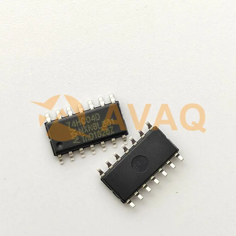
74HC04D
Toshiba
5000+ $0,072
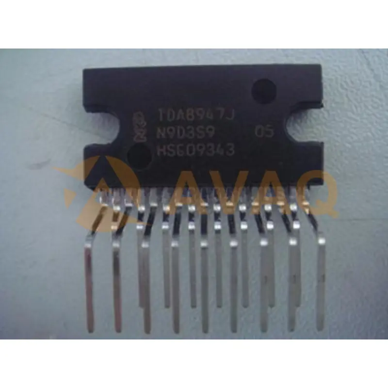
TDA8947J
NXP
Audio Amplifiers 3/4 CHANNEL AUDIO AMPLIFIER
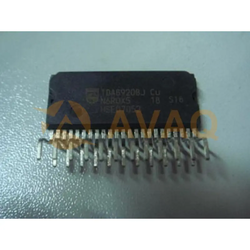
TDA8920BJ
Nxp
Experience crystal-clear sound quality and robust power handling with this efficient Class D amplifier
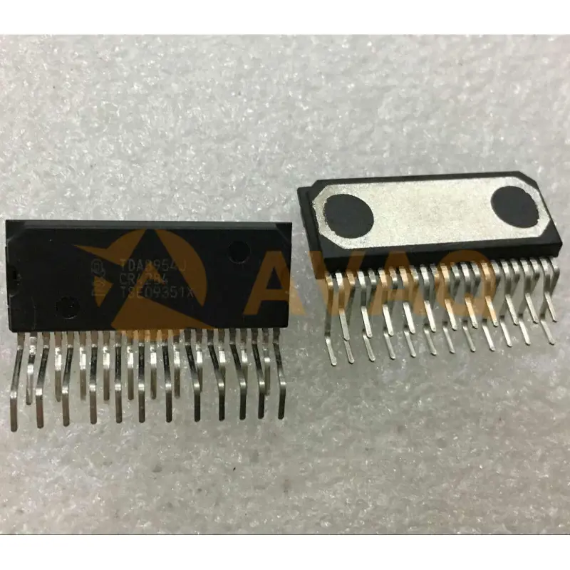
TDA8954J
Nxp
Plastic SOT411-1 PZFM23 audio amplifier
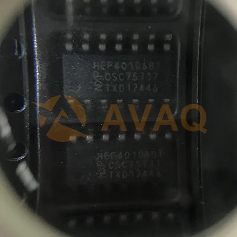
HEF40106BT
Nexperia
Inverter Schmitt Trigger 6-Element CMOS 14-Pin SO
