Metodo di pagamento


ARM926EJ-S Microprocessor IC OMAP-L1x 1 Core, 32-Bit 375MHz 256-BGA (17x17)
Produttore:
ProduttorePart #:
OMAPL137DZKBA3
Scheda dati:
Series:
OMAP-L1x
Core Processor:
ARM926EJ-S
Number of Cores/Bus Width:
1 Core, 32-Bit
Speed:
375MHz
EDA/CAD Modelli:
Compila il breve modulo sottostante e ti forniremo immediatamente il preventivo.
The OMAP-L137 device is a low-power applications processor based on an ARM926EJ-S and a TMS320C674x DSP core. It consumes significantly lower power than other members of the TMS320C6000 platform of DSPs.
The OMAP-L137 device enables original-equipment manufacturers (OEMs) and original-design manufacturers (ODMs) to quickly bring to market devices featuring robust operating systems support, rich user interfaces, and high processing performance life through the maximum flexibility of a fully integrated mixed processor solution.
The dual-core architecture of the OMAP-L137 device provides benefits of both DSP and Reduced Instruction Set Computer (RISC) technologies, incorporating a high-performance TMS320C674x DSP core and an ARM926EJ-S core.
The ARM926EJ-S is a 32-bit RISC processor core that performs 32-bit or 16-bit instructions and processes 32-bit, 16-bit, or 8-bit data. The core uses pipelining so that all parts of the processor and memory system can operate continuously.
The ARM core has a coprocessor 15 (CP15), protection module, and data and program Memory Management Units (MMUs) with table look-aside buffers. The ARM core has separate 16-KB instruction and 16KB of data caches. Both memory blocks are four-way associative with virtual index virtual tag (VIVT). The ARM core also has 8KB of RAM (Vector Table) and 64KB of ROM.
The OMAP-L137 DSP core uses a two-level cache-based architecture. The Level 1 program cache (L1P) is a 32-KB direct mapped cache and the Level 1 data cache (L1D) is a 32-KB 2-way set-associative cache. The Level 2 program cache (L2P) consists of a 256-KB memory space that is shared between program and data space. L2 memory can be configured as mapped memory, cache, or combinations of the two. Although the DSP L2 is accessible by ARM and other hosts in the system, an additional 128KB of RAM shared memory is available for use by other hosts without affecting DSP performance.
The peripheral set includes: a 10/100 Mbps Ethernet MAC (EMAC) with a management data input/output (MDIO) module; two I2C Bus interfaces; 3 multichannel audio serial ports (McASPs) with 16/12/4 serializers and FIFO buffers; two 64-bit general-purpose timers each configurable (one configurable as watchdog); a configurable 16-bit host-port interface (HPI); up to 8 banks of 16 pins of general-purpose input/output (GPIO) with programmable interrupt/event generation modes, multiplexed with other peripherals; 3 UART interfaces (one with both RTS and CTS); three enhanced high-resolution pulse width modulator (eHRPWM) peripherals; three 32-bit enhanced capture (eCAP) module peripherals which can be configured as 3 capture inputs or 3 auxiliary pulse width modulator (APWM) outputs; two 32-bit enhanced quadrature encoded pulse (eQEP) peripherals; and 2 external memory interfaces: an asynchronous and SDRAM external memory interface (EMIFA) for slower memories or peripherals, and a higher speed memory interface (EMIFB) for SDRAM.
The Ethernet Media Access Controller (EMAC) provides an efficient interface between the OMAP-L137 device and the network. The EMAC supports both 10Base-T and 100Base-TX, or 10 Mbps and 100 Mbps in either half- or full-duplex mode. Additionally, an MDIO interface is available for PHY configuration.
The HPI, I2C, SPI, USB1.1, and USB2.0 ports allow the OMAP-L137 device to easily control peripheral devices and/or communicate with host processors.
The rich peripheral set provides the ability to control external peripheral devices and communicate with external processors. For details on each of the peripherals, see the related sections later in this document and the associated peripheral reference guides.
The OMAP-L137 device has a complete set of development tools for both the ARM and DSP. These include C compilers, a DSP assembly optimizer to simplify programming and scheduling, and a Windows® debugger interface for visibility into source code execution.
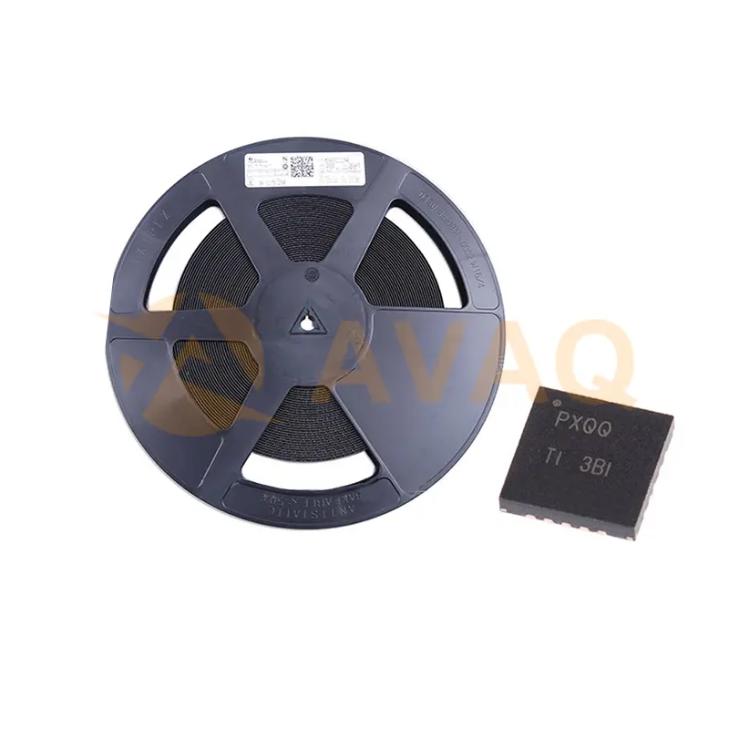
| Category | Integrated Circuits (ICs)EmbeddedMicroprocessors | Series | OMAP-L1x |
| Core Processor | ARM926EJ-S | Number of Cores/Bus Width | 1 Core, 32-Bit |
| Speed | 375MHz | Co-Processors/DSP | Signal Processing; C674x, System Control; CP15 |
| RAM Controllers | SDRAM | Graphics Acceleration | No |
| Display & Interface Controllers | LCD | Ethernet | 10/100Mbps (1) |
| SATA | - | USB | USB 1.1 + PHY (1), USB 2.0 + PHY (1) |
| Voltage - I/O | 1.8V, 3.3V | Operating Temperature | -40°C ~ 105°C (TJ) |
| Security Features | - | Mounting Type | Surface Mount |
| Additional Interfaces | HPI, I²C, McASP, MMC/SD, SPI, UART | Base Product Number | OMAPL137 |
| Arm CPU | 1 Arm9 | Arm (max) (MHz) | 456 |
| Coprocessors | C674x DSP | CPU | 32-bit |
| Display type | 1 LCD | Protocols | Ethernet |
| Ethernet MAC | 1-Port 10/100 | Hardware accelerators | PRUSS |
| Operating system | Linux, RTOS | Security | Device identity, Memory protection |
| Rating | Catalog | Power supply solution | TPS65910 |
| Operating temperature range (°C) | -40 to 105, -40 to 125, -40 to 90, 0 to 90 |
Relativi al servizio post-vendita e alla liquidazione
 Pagamento
Metodo di pagamento


Per canali di pagamento alternativi, contattaci a:
[email protected] Spedizione e imballaggio
metodo di spedizione


AVAQ determina e confeziona tutti i dispositivi in base ai requisiti di protezione contro le scariche elettrostatiche (ESD) e il livello di sensibilità all'umidità (MSL)..
 Garanzia

Prodotto 365 giorni
Qualità garantita
Promettiamo di fornire un servizio di garanzia della qualità di 365 giorni per tutti i nostri prodotti.
| Qtà. | Prezzo unitario | Est. Prezzo |
|---|---|---|
| 1+ | $14,718 | $14,72 |
| 10+ | $14,132 | $141,32 |
| 30+ | $13,117 | $393,51 |
| 100+ | $12,231 | $1.223,10 |
I prezzi sottostanti sono solo di riferimento.
Tutte le distinte materiali (BOM) possono essere inviate via e-mail a ![]() [email protected],
oppure compila il modulo sottostante per effettuare un preventivo per OMAPL137DZKBA3, preventivi garantiti entro
[email protected],
oppure compila il modulo sottostante per effettuare un preventivo per OMAPL137DZKBA3, preventivi garantiti entro
![]() 12 ore.
12 ore.
AM3358BZCZ100
TI
126+ $8,358
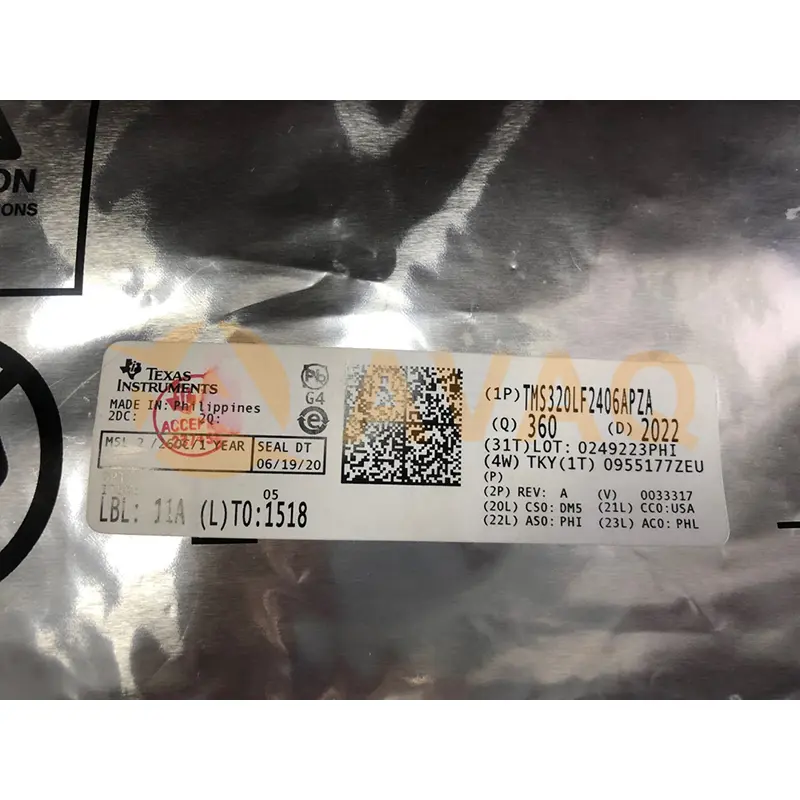
TMS320LF2406APZA
Texas Instruments
100+ $7,554
MSP430FR5969
TI
16 MHz MCU with 64KB FRAM, 2KB SRAM, AES, 12-bit ADC, comparator, DMA, UART/SPI/I2C, timer
TMS320C6713
TI
FLOATING-POINTDIGITALSIGNALPROCESSORS
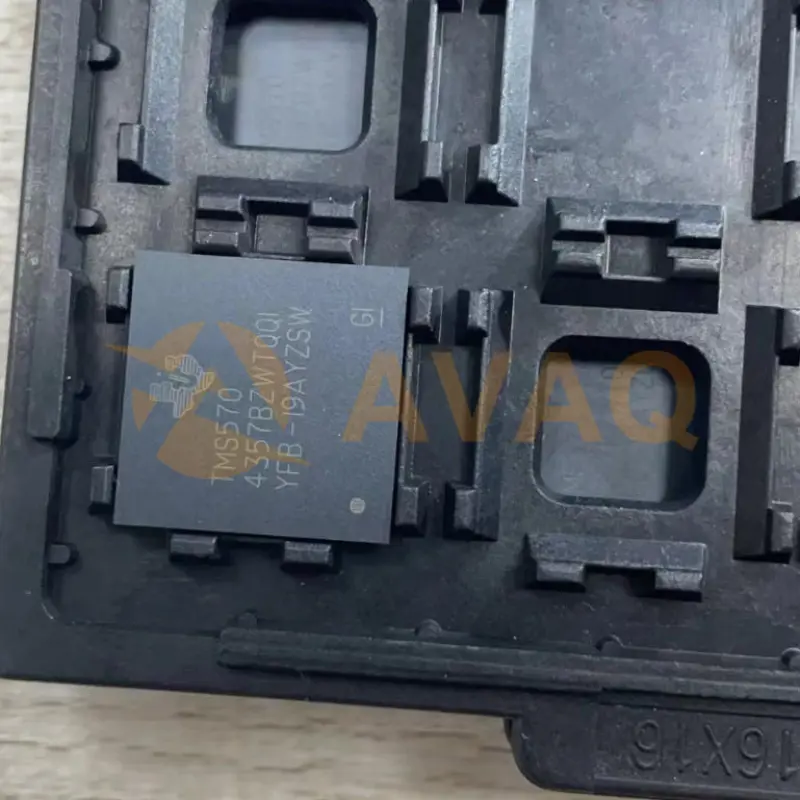
TMS5704357BZWTQQ1
Texas Instruments, Inc
MCU 32-bit ARM Cortex R5F RISC 4MB Flash 1.2V/3.3V Automotive 337-Pin NFBGA Tray