Metodo di pagamento


MachXO series device operating at 1.8V, 2.5V, or 3.3V
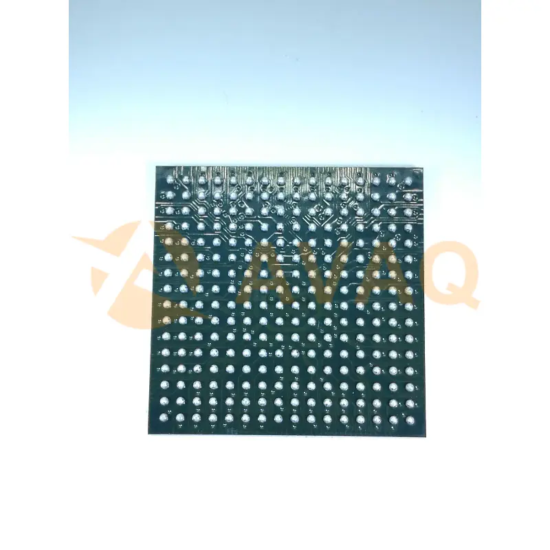
CSBGA-256Produttore:
Lattice Semiconductor Corporation
ProduttorePart #:
LCMXO640C-3FTN256C
Scheda dati:
Programmabe:
Not Verified
Number Of LABs/CLBs:
80
Number Of Logic Elements/Cells:
640
Number Of I/O:
159
EDA/CAD Modelli:
All bill of materials (BOM) can be sent via email to ![]() [email protected],
or fill below form to Quote for LCMXO640C-3FTN256C, guaranteed quotes back within
[email protected],
or fill below form to Quote for LCMXO640C-3FTN256C, guaranteed quotes back within
![]() 12hr.
12hr.
Compila il breve modulo sottostante e ti forniremo immediatamente il preventivo.
The LCMXO640C-3FTN256C from Lattice Semiconductor is a versatile FPGA IC designed for high-volume applications in the consumer, communication, and industrial markets. With 640 LUTs, 32Kbits of embedded SRAM, and 48 user I/Os, this low-cost, low-power device offers a range of features to support complex system designs. It operates at a speed grade of 3 and comes in a 256-pin fine-pitch BGA package, making it suitable for demanding applications where both performance and compactness are essential. The non-volatile configuration memory ensures that the FPGA can retain its configuration even when powered off, simplifying the overall system design by eliminating the need for external configuration memory. Additionally, the LCMXO640C-3FTN256C supports advanced features such as Clock Conditioning Circuits (CCC), Phase-Locked Loops (PLLs), and built-in JTAG programming, providing flexibility and ease of use in device configuration. As such, the LCMXO640C-3FTN256C is an ideal choice for designers looking to achieve high performance and functionality in a cost-effective and power-efficient manner
| Programmabe | Not Verified | Number of LABs/CLBs | 80 |
| Number of Logic Elements/Cells | 640 | Total RAM Bits | - |
| Number of I/O | 159 | Number of Gates | - |
| Voltage - Supply | 1.71V ~ 3.465V | Mounting Type | Surface Mount |
| Operating Temperature | 0°C ~ 85°C (TJ) |
Relativi al servizio post-vendita e alla liquidazione
 Pagamento
Metodo di pagamento


Per canali di pagamento alternativi, contattaci a:
[email protected] Spedizione e imballaggio
metodo di spedizione


AVAQ determina e confeziona tutti i dispositivi in base ai requisiti di protezione contro le scariche elettrostatiche (ESD) e il livello di sensibilità all'umidità (MSL)..
 Garanzia

Prodotto 365 giorni
Qualità garantita
Promettiamo di fornire un servizio di garanzia della qualità di 365 giorni per tutti i nostri prodotti.
| Qtà. | Prezzo unitario | Est. Prezzo |
|---|---|---|
| 1+ | $18,797 | $18,80 |
| 200+ | $7,274 | $1.454,80 |
| 500+ | $7,019 | $3.509,50 |
| 1000+ | $6,892 | $6.892,00 |
I prezzi sottostanti sono solo di riferimento.

C100
Issi
Video ICs 4MP H.265 Video Processor - 64MB DDR2, BGA85, 5mm x 6mm
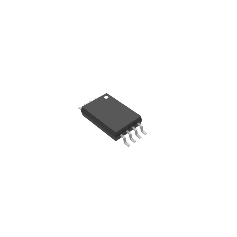
NE555
Texas Instruments
100kHz operation frequency with low power consumption for long-lasting performance
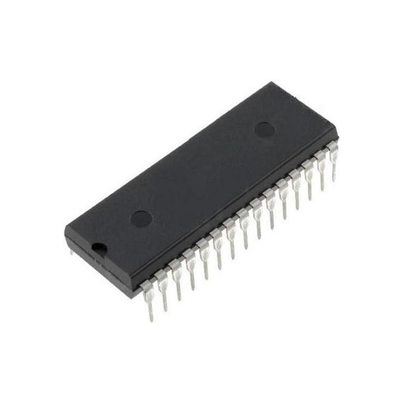
CD4017
Onsemi
Compact digital counter for precision measurement application

74LS04
Onsemi
High-quality die for professional use only, unsurfaced and untested
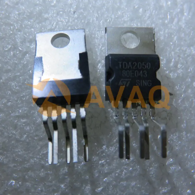
TDA2050
Stmicroelectronics
Effortlessly drives your speakers with crystal-clear sound and robust power
