EP1S40F780C7N Descrizione generale
Harnessing the power of 40,000 logic elements and 780Kbits of embedded memory, the EP1S40F780C7N FPGA by Altera is a cutting-edge solution for high-performance applications. Built on a 90nm processing technology, this FPGA excels in handling complex logic functions, signal processing, and connectivity requirements. With 7,680 logic array blocks and 280 embedded multipliers, it offers remarkable processing capabilities, operating at a maximum internal frequency of 260MHz. Supporting various communication protocols like PCI Express, Gigabit Ethernet, and SATA, the EP1S40F780C7N is the ideal choice for applications that demand superior performance and reliability
Caratteristiche principali
Configuration devices for SRAM-based LUT devices offer the following features:
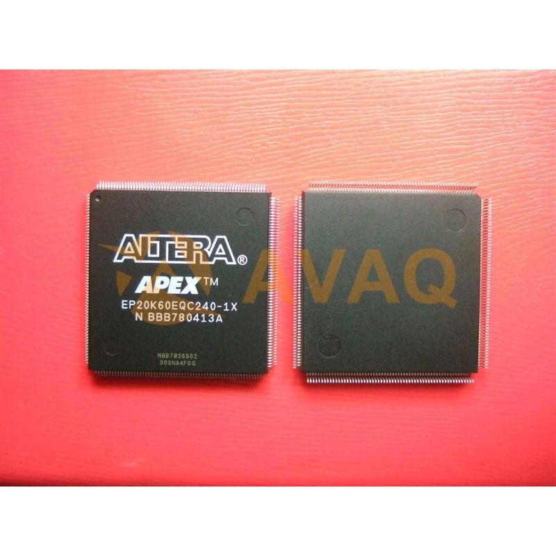
Configures Altera ACEX 1K, APEX 20K (including APEX 20K, APEX 20KC, and APEX 20KE), APEX II, Arria GX, Cyclone, Cyclone II, FLEX 10K (including FLEX 10KE and FLEX 10KA) Mercury, Stratix, Stratix GX, Stratix II, and Stratix II GX devices
Easy-to-use four-pin interface
Low current during configuration and near-zero standby mode current
Programming support with the Altera Programming Unit (APU) and programming hardware from Data I/O, BP Microsystems, and other third-party programmers
Available in compact plastic packages
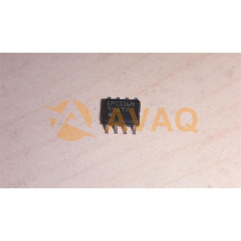
8-pin plastic dual in-line (PDIP) package
20-pin plastic J-lead chip carrier (PLCC) package
32-pin plastic thin quad flat pack (TQFP) package
EPC2 device has reprogrammable flash configuration memory
5.0-V and 3.3-V in-system programmability (ISP) through the built-in IEEE Std.
1149.1 JTAG interface
Built-in JTAG boundary-scan test (BST) circuitry compliant with IEEE Std. 1149.1
Supports programming through Serial Vector Format File (.svf), Jam Standard Test and Programming Language (STAPL) Format File (.jam), JAM Byte Code File (.jbc), and the Quartus II and MAX+PLUS II softwares using the USB-Blaster, MasterBlaster, ByteBlaster II, EthernetBlaster, or ByteBlasterMV download cable
Supports programming through Programmer Object File (.pof) for EPC1 and EPC1441 devices
nINIT_CONF pin allows INIT_CONF JTAG instruction to begin FPGA configuration


 Pagamento


 Spedizione e imballaggio


 Garanzia