Metodo di pagamento


130nm Technology
PQFP-208Produttore:
MICROCHIP TECHNOLOGY INC
ProduttorePart #:
A3PE3000-PQG208I
Scheda dati:
Part Life Cycle Code:
Active
Reach Compliance Code:
compliant
HTS Code:
8542.39.00.01
Factory Lead Time:
52 Weeks
EDA/CAD Modelli:
Invia tutte le distinte materiali a ![]() [email protected],
oppure compila il modulo sottostante per un preventivo su A3PE3000-PQG208I. Risposta garantita entro
[email protected],
oppure compila il modulo sottostante per un preventivo su A3PE3000-PQG208I. Risposta garantita entro
![]() 12hr.
12hr.
Compila il breve modulo sottostante e ti forniremo immediatamente il preventivo.
Designed with security in mind, the A3PE3000-PQG208I includes advanced features such as tamper detection, secure key storage, and anti-tamper mesh, ensuring that your sensitive data remains protected at all times. The FPGA also supports multiple I/O standards, making it easy to integrate into existing systems and interfaces. The RoHS compliant 208-pin plastic quad flat package (PQG208) is durable and easy to work with, giving you peace of mind knowing that your components meet strict environmental standards
High Capacity
600 k to 3 Million System Gates
108 to 504 kbits of True Dual-Port SRAM
Up to 620 User I/Os
Reprogrammable Flash Technology
130-nm, 7-Layer Metal (6 Copper), Flash-Based CMOS Process
Instant On Level 0 Support
Single-Chip Solution
Retains Programmed Design when Powered Off
On-Chip User Nonvolatile Memory
1 kbit of FlashROM with Synchronous Interfacing
High Performance
350 MHz System Performance
3.3 V, 66 MHz 64-Bit PCI
In-System Programming (ISP) and Security
ISP Using On-Chip 128-Bit Advanced Encryption Standard (AES) Decryption via JTAG (IEEE 1532compliant)
FlashLock Designed to Secure FPGA Contents
Low Power
Core Voltage for Low Power
Support for 1.5-V-Only Systems
Low-Impedance Flash Switches
High-Performance Routing Hierarchy
Segmented, Hierarchical Routing and Clock Structure
Ultra-Fast Local and Long-Line Network
Enhanced High-Speed, Very-Long-Line Network
High-Performance, Low-Skew Global Network
Architecture Supports Ultra-High Utilization
Pro (Professional) I/O
700 Mbps DDR, LVDS-Capable I/Os
1.5 V, 1.8 V, 2.5 V, and 3.3 V Mixed-Voltage Operation
Bank-Selectable I/O Voltagesup to 8 Banks per Chip
Single-Ended I/O Standards: LVTTL, LVCMOS 3.3 V / 2.5 V / 1.8 V / 1.5 V, 3.3 V PCI / 3.3 V PCI-X, and LVCMOS 2.5 V / 5.0 V Input
Differential I/O Standards: LVPECL, LVDS, B-LVDS, and M-LVDS
Voltage-Referenced I/O Standards: GTL+ 2.5 V / 3.3 V, GTL 2.5 V / 3.3 V, HSTL Class I and II, SSTL2 Class I and II, SSTL3 Class I and II
I/O Registers on Input, Output, and Enable Paths
Hot-Swappable and Cold Sparing I/Os
Programmable Output Slew Rate and Drive Strength
Programmable Input Delay
Schmitt Trigger Option on Single-Ended Inputs
Weak Pull-Up/-Down
IEEE 1149.1 (JTAG) Boundary Scan Test
Pin-Compatible Packages across the ProASIC3E Family
Clock Conditioning Circuit (CCC) and PLL
Six CCC Blocks, Each with an Integrated PLL
Configurable Phase-Shift, Multiply/Divide, Delay Capabilities and External Feedback
Wide Input Frequency Range (1.5 MHz to 350 MHz)
SRAMs and FIFOs
Variable-Aspect-Ratio 4,608-Bit RAM Blocks (1, 2, 4, 9, and 18 organizations available)
True Dual-Port SRAM (except 18)
24 SRAM and FIFO Configurations with Synchronous Operation up to 350 MHz
ARM Processor Support in ProASIC3E FPGAs
M1 ProASIC3E DevicesCortex-M1 Soft Processor Available with or without Debug
| Part Life Cycle Code | Active | Reach Compliance Code | compliant |
| HTS Code | 8542.39.00.01 | Factory Lead Time | 52 Weeks |
| JESD-30 Code | S-PQFP-G208 | JESD-609 Code | e3 |
| Length | 28 mm | Moisture Sensitivity Level | 3 |
| Number of CLBs | 75264 | Number of Equivalent Gates | 3000000 |
| Number of Inputs | 147 | Number of Logic Cells | 75264 |
| Number of Outputs | 147 | Number of Terminals | 208 |
| Operating Temperature-Max | 85 °C | Operating Temperature-Min | -40 °C |
| Organization | 75264 CLBS, 3000000 GATES | Peak Reflow Temperature (Cel) | 245 |
| Power Supplies | 1.5/3.3 V | Programmable Logic Type | FIELD PROGRAMMABLE GATE ARRAY |
| Qualification Status | Not Qualified | Seated Height-Max | 4.1 mm |
| Supply Voltage-Max | 1.575 V | Supply Voltage-Min | 1.425 V |
| Supply Voltage-Nom | 1.5 V | Surface Mount | YES |
| Technology | CMOS | Temperature Grade | INDUSTRIAL |
| Terminal Finish | MATTE TIN | Terminal Form | GULL WING |
| Terminal Pitch | 0.5 mm | Terminal Position | QUAD |
| Time@Peak Reflow Temperature-Max (s) | 30 | Width | 28 mm |
Relativi al servizio post-vendita e alla liquidazione
 Pagamento
Metodo di pagamento


Per canali di pagamento alternativi, contattaci a:
[email protected] Spedizione e imballaggio
metodo di spedizione


AVAQ determina e confeziona tutti i dispositivi in base ai requisiti di protezione contro le scariche elettrostatiche (ESD) e il livello di sensibilità all'umidità (MSL)..
 Garanzia

Prodotto 365 giorni
Qualità garantita
Promettiamo di fornire un servizio di garanzia della qualità di 365 giorni per tutti i nostri prodotti.
| Qtà. | Prezzo unitario | Est. Prezzo |
|---|---|---|
| 1+ | - | - |
I prezzi sottostanti sono solo di riferimento.
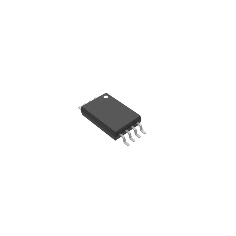
NE555
Texas Instruments
100kHz operation frequency with low power consumption for long-lasting performance
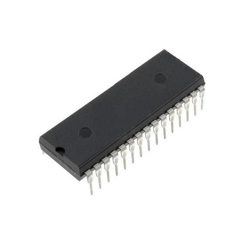
CD4017
Onsemi
Compact digital counter for precision measurement application

74LS04
Onsemi
High-quality die for professional use only, unsurfaced and untested
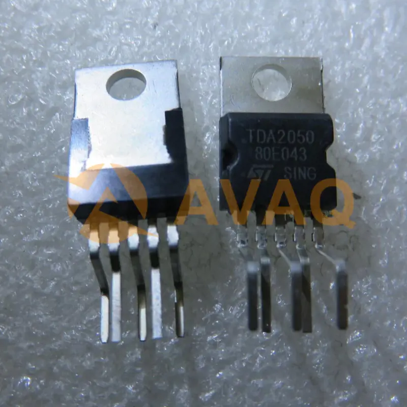
TDA2050
Stmicroelectronics
Effortlessly drives your speakers with crystal-clear sound and robust power
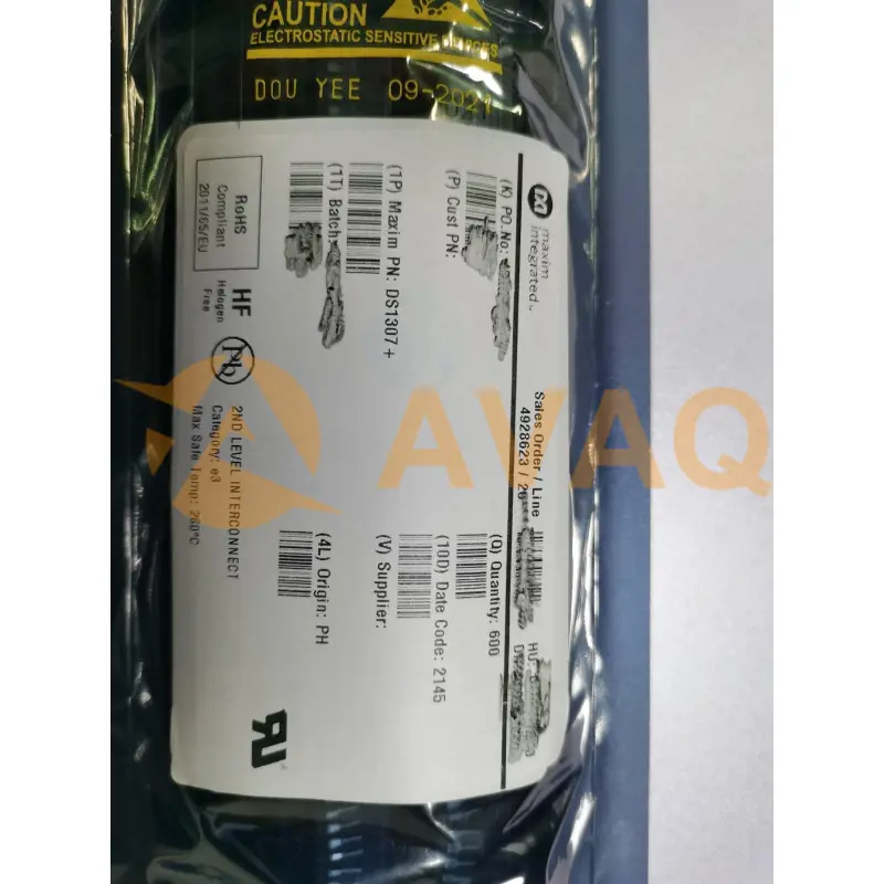
DS1307+
Analog Devices
I2C DIP-8 Real-time Clocks (RTC) ROHS