Different Parts of Optical Crystal Triode
 Pubblicato: Apr 27, 2023
Contents
Optical Crystal Triode
Optical crystal triode is composed of dual auroral electric transistor, optical field effect phototransistor and its related devices.
Light is absorbed in the active region of these devices, generating photogenerated carriers that produce photocurrent gain through an internal electrical amplification mechanism. Phototransistors work at three ends, so they are easy to realize electric control or electric synchronization.
Construction of Optical Crystal Triode
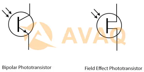
Bipolar Phototransistors
Bipolar type phototransistors are structurally divided into homogeneous and heterogeneous types. The figure shows the energy band diagram of heterojunction phototransistor. Light is absorbed in the base-collector region and the resulting holes (multiplets) accumulate in the base-region, causing the emitter junction to inject more electrons to maintain electrical neutrality and generate gain. Compared with the homogeneous junction type, it has the following advantages: (1) the use of broadband emission region as the optical window greatly improves the quantum efficiency. For short wavelengths (shorter than 0.9 µm), GaAs-GaAlAs systems are commonly used, while for long wavelengths (longer than 1.1 µm), InP-InGaAsP systems are used. For the latter, backside illumination can also be used. These systems are based on direct energy gap semiconductor, high light absorption, so it can be made thinner, greatly reducing the base area transition time.
Bipolar phototransistor usually has high gain, but the speed is not too fast, for GaAs-GaAlAs, β can be greater than 1000, the response time is greater than nanoseconds (depending on the size of the gain varies). The gain bandwidth product GB is limited by the emitter and collector charging time constants at low current and weak illumination; while at high current or strong illumination, it is basically determined by the base region crossing time and collector crossing time. Generally (Figure 1), fT is the transistor cut-off frequency. The GaAs-GaAlAs phototransistor response time is 250 picoseconds or less.
The noise of heterojunction phototransistor is determined by the operating current, which is lower at low current. However, the emitter time constant increases at low current operation, and the space charge region complex flow dominates the component, which also causes the gain reduction (β is proportional to, Ie,n≈2). In order to reduce the space charge region complex flow, molecular beam epitaxy can be used to grow a broadband base region of about 300Å at one end of the emitter junction and form part of the space charge region in the base region, which is the "double base region" structure.
Heterojunction phototransistors are used in photodetectors, and their performance is not inferior to that of PIN photodiodes and field-effect compound systems, and they can also be used for optical amplification.
Field Effect Transistor (FET)
Field Effect Transistor (FET) is abbreviated as Field Effect Transistor. There are two main types: junction FET (Junction FET-JFET) and metal-oxide semiconductor FET (MOS-FET). Conducted by a majority of carriers, it is also called a unipolar transistor. It is a voltage-controlled semiconductor device. With the advantages of high input resistance (107 to 1015Ω), low noise, low power consumption, large dynamic range, easy integration, no secondary breakdown phenomenon, and wide safe working area, it has become a strong competitor of bipolar transistors and power transistors.
Field effect tube (FET) is a semiconductor device that uses the electric field effect of the control input circuit to control the output circuit current, and is named as such.
It is also known as a unipolar transistor because it conducts only by the majority of carriers in the semiconductor.
Optical Field-Effect Transistors and Related Optoelectronic Devices
GaAs MESFETs can be used as very high-speed photodetectors (GaAs op FETs) with response times of 50 picoseconds or less and gains greater than 10 (depending on operating conditions). The disadvantage is that the photosensitive area is small.
GaAs op FET and its related N-channel optoelectronic devices have optical gain mechanism:
① photoheterodyne mechanism, the gain is equal to the ratio of electron velocity to hole velocity.
② transfer electron effect mechanism, the gain comes from the space charge amplification of photogenerated carriers in the negative mobility region. Related to this there are many other planar optoelectronic devices, which are characterized by fast speed (response time tens of picoseconds), suitable for integration.
Prossimo focus sul settore
What is the Classification of Mechanical Comparators?
 Tempo di aggiornamento: Apr 28, 2023 Elettronica di consumo
 Focus del settore popolare
Hot Products
-
![TMP01ES]()
TMP01ES
Analog Devices Inc.
SOIC N tube packaging contains an 8-pin analog temperature sensor
-
![LT8608IMSE]()
LT8608IMSE
ADI
High frequency operation for improved efficiency
-
![DS2438Z+T&R]()
DS2438Z+T&R
ADI
Li-Ion Battery Monitor
-
![MAX3491ESD+T]()
MAX3491ESD+T
ADI
Integrated circuit suitable for industrial applications
-
![OP400HS]()
OP400HS
Analog Devices Inc.
Quad Amp with Bipolar Technology
-
![MAX187BCPA]()
MAX187BCPA
ADI
Compact 8-pin PDIP package ideal for space-constrained designs


Parti correlate
-
![Hi3556V100]()
Hi3556V100
HISILICON
-
![Si7686DP]()
Si7686DP
VISHAY
N-Ch. Reduced Qg, Fast Switching MOSFET; PWM optimized;
-
![SiR880DP]()
SiR880DP
VISHAY
N-Channel 80 V (D-S) MOSFET 100 % UIS Tested
-
![SI1080]()
SI1080
VISHAY
Proprietary Si10xx Sub-GHz Wireless MCPs
-
![H26M31002GPR]()
H26M31002GPR
SKHYNIX
4GB eMMC Nand Flash
-
![XE1401]()
XE1401
SEMTECH
Multi-National 14,400 BPS Embeddable Modem
-
![RTL8197FNT]()
RTL8197FNT
REALTEK
-
![MSM6290]()
MSM6290
QUALCOMM
-
![NJW1157]()
NJW1157
JRC
8-CHANNEL ELECTRONIC VOLUME WITH INPUT SELECTOR
-
![AUO-M201-20]()
AUO-M201-20
AUO
-
![AM79C972]()
AM79C972
AMD
PCnet⑩-FAST+ Enhanced 10/100 Mbps PCI Ethernet Controller with OnNow Support
-
![AM29040]()
AM29040
AMD
Am29040? Processor Data Sheet
-
![9PC8666X-S001]()
9PC8666X-S001
SANYO DENKI
Fan PWM Controller For
-
![ASP-161801-01]()
ASP-161801-01
SAMTEC

Featured Manufacturers